Just received my 2W IR laser, as promised mid-July, so very happy! Setup is straightforward. For those who found the pages of Snapmaker confusing, regarding if you need the QSK adapter plate or not (I found them confusing…): You do not need it, the profile on the laser’s back is ready for the Snapmaker 2.0 QSK. I like that!
Focusing with the focus lever is totally straightforward: simple, but effective. My anxiety is that the lever might get lose, bump on the workpiece and get tangled - but that is me, just seeing the bad things ![]() I suppose if that was an issue, we would have heard of similar problems with the 20/40W lasers, that use the same method.
I suppose if that was an issue, we would have heard of similar problems with the 20/40W lasers, that use the same method.
Work origin with crosshairs is very easy, nice. Not yet checked how precise it aligns with the actual laser, but I guess it will be sufficient.
After scorching some wood as a first test, I jumped directly at PCB board, because that’s what I hope I’ll use the 2W thing most for. First surprise: The laser is not completely invisible - obviously the side-waves reach into the visible spectrum. or it’s the evaporating, hot material, not sure.
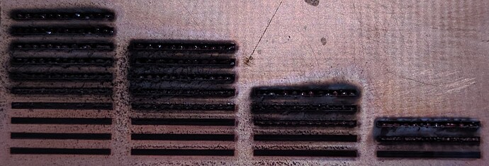
I yet did not have full success with PCB. The laser is certainly able to get the copper away, but somehow it does not achieve full isolation. Right after the laser process, there is close to 0 Ohm between the two sides of an isolation line, i.e. no isolation at all. After polishing the copper and laser-cut a bit, resistance goes up to ~10-100 Ohms - still not good. If I then use a knife to trace the isolation routes and scratch out all the soot from the PCB base plate, I finally get to full isolation, but that’s not a feasible process for a larger PCB. My guess is that the soot is conductive (carbon is). So I’ll need to try more parameter sets in the sense of speed & passes. My first tries were going very slow (10-25 mm/min!), but this seems to damage the PCB carrier material too much. Going at 200 mm/min on the other hand is not ablating the copper efficiently. So, still parameters need to be worked out, but I guess I’ll get there eventually. What is already clear is: It will not be a fast process to laser-etch a PCB.
@Zoe @Jade will you share best practice values for PCB isolation routing at some point? It seems a really tedious process to work it out, and I guess help would be appreciated!
What certainly is remarkable is how unbelievable fine the focus is! The lines are sooo thin, and when I set the line spacing too high, I had very tiny strands of copper remaining between the burnt away copper. From the Lightburn numbers, I’d say the laser cut lines are less than 0.1 mm, perhaps even less than 0.05 mm. I guess this device will be able to engrave ubelievably intricate patterns!
So first impression is good, especially the tiny focus is promising!
Here are photos of my first tries (sorry for the typos - did not properly control the image before upload…):
The underside shows how the heat damages the carrier material when going slow (10-25 mm/min):


